
01 / QUANTUMQX / PQX
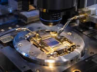
Quantum Error Control
코히어런트 인과순서와 오류응답 구조를 탐구하며, 양자 연산의 신뢰성을 향상시킬 수 있는 수학적·물리적 경로를 연구합니다.
COHERENCE / ERROR RESPONSE / VALIDATION
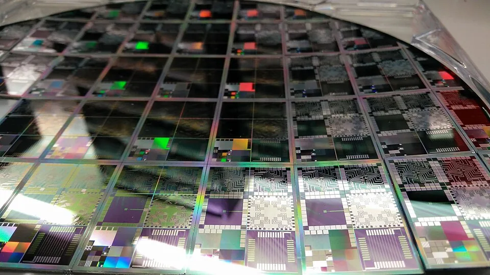
양자 오류제어, 광자 반도체 소자, 그리고 신뢰할 수 있는 차세대 연산 구조. 에버노바랩스는 빛의 물리학을 정밀한 엔지니어링과 검증 가능한 기술로 연결합니다.
빛은 정보를 운반하는 매개체를 넘어, 연산·제어·측정을 새롭게 설계할 수 있는 물리적 플랫폼입니다. 우리는 양자와 광자의 기초 원리를 설계, 제조 가능성, 계측과 재현성까지 잇는 연구체계를 구축합니다.
양자 오류제어에서 광자 소자, 통신 제어코어와 칩 통합까지. 각 연구 트랙의 목표와 검증 단계를 구분해 발전시킵니다.
코히어런트 인과순서와 오류응답 구조를 탐구하며, 양자 연산의 신뢰성을 향상시킬 수 있는 수학적·물리적 경로를 연구합니다.
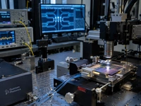
집적 광회로(PIC), 단일광자 방출체와 연속체 내 속박상태(BIC) 결합을 포함한 광자소자 아키텍처를 연구합니다.
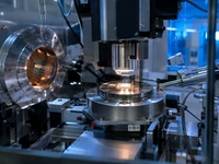
공통 CMOS 제어코어, 물리계층 송출 제어, 증거 기반 통신경로 승인과 선택형 광자회로 결합을 함께 설계·평가합니다.
소자별 특성 측정과 편차 분석을 바탕으로 조합, 패키징, 재시험과 제조 적합성 평가를 연계합니다.
EVERNOVA / FRONTIER PORTFOLIO
Research-led exploration of quantum photonics, communication silicon, next-generation materials and embodied artificial intelligence.
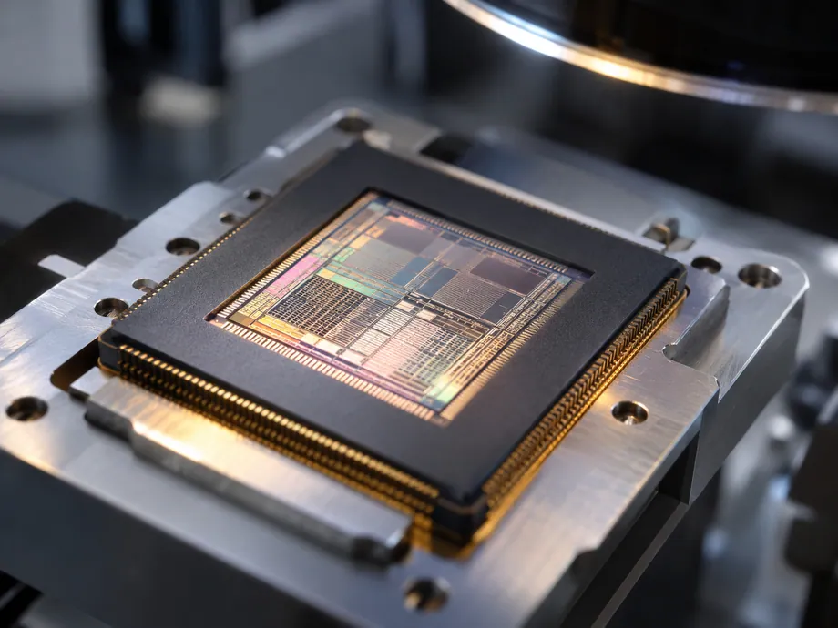
Communications semiconductor research for 5G-Advanced and NTN interoperability, future 6G pathways and Physical AI mobility across terrestrial, maritime and aerial environments.
APPLICATIONS ↗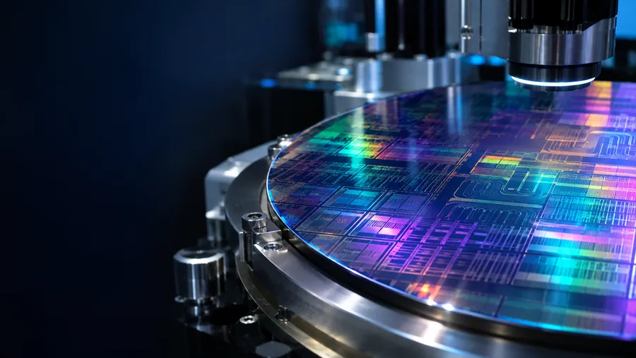
Quantum-error-control concepts, photonic integrated circuits, advanced optical devices and measurement-driven semiconductor research.
RESEARCH ↗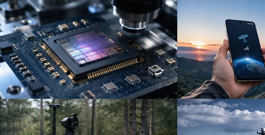
Exploratory research into advanced superconducting-material candidates, physical plausibility, materials screening and repeatable experimental validation.
VALIDATION ↗PHYSICAL AI / RESILIENT MOBILITY
Future-oriented research exploring human-form Physical AI, robotic teams and connectivity in complex operating environments.

Human-form and mobile robot platforms for hazardous environments, sensor-to-edge coordination and supervised autonomy.
UAVs, maritime robotics and cross-domain data connectivity as prospective application areas.
Security research aimed at detecting cyber interference, jamming, spoofing and loss of network service, with controlled fallback and recovery.
QPX × NTN MOBILITY CONNECTIVITY
Exploring internal NTN modem and antenna integration in familiar smartphone form factors. Five operating environments illustrate potential research applications.
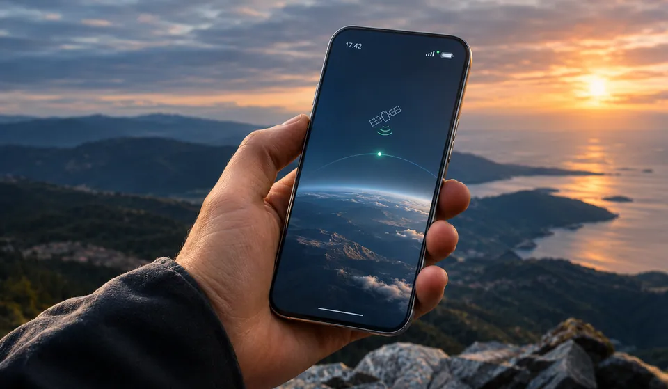




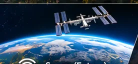
Future orbital applications would require additional capabilities. All scenes are conceptual, not field tests or product certifications.
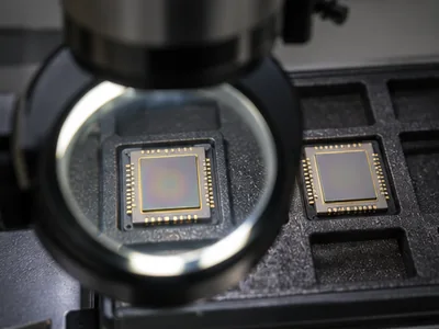
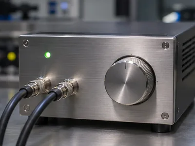
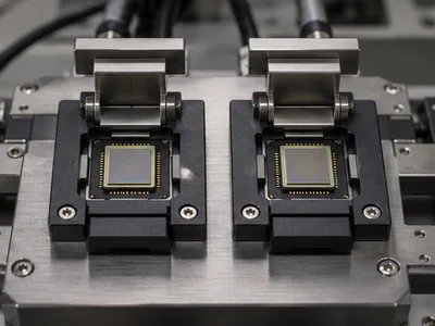
웨이퍼 미세구조, 광학 실험장치, 클린룸 제조 공정. 현대 반도체와 광자 연구의 실제 모습을 참고사진으로 소개합니다.
공개 참고사진 · 에버노바 소유 시설의 사진이 아닙니다. 사진 출처와 라이선스는 하단에 명시했습니다.
물리 원리와 제조 제약, 측정 신뢰도를 하나의 연구 흐름으로 결합합니다. 단계별 실험 결과를 다음 설계에 반영하는 구조입니다.
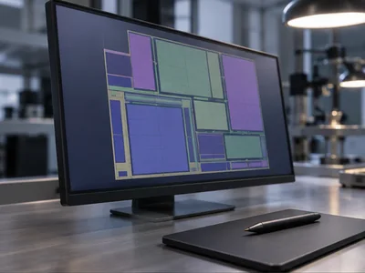
설계·가설
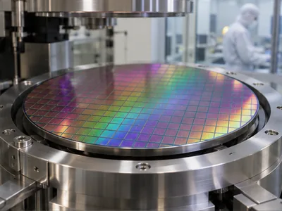
제조 검토
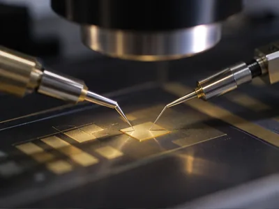
물리 측정
증거 평가
실행 제어
독립 재검증
광자 소자와 양자 반도체의 설계·제조·계측 과정을 영화적 언어로 표현한 EverNova Labs 기술 비전 영상입니다.
EverNova Labs는 광자반도체 파운드리, 대학·연구기관, 계측·패키징 전문가와 함께 연구의 다음 단계를 연결하는 협력을 지향합니다.
수석연구부소장 / Deputy Director, Research
연구기관, 파운드리, 광자 소자 개발사, 측정·평가 기관과의 기술교류 및 단계별 공동연구를 모색합니다.
상업화·글로벌 고객 서비스는 KINGDOM INTELLIGENCE에서 별도로 안내합니다.
kingdomintelligence.global ↗